GPIO of Beaglebone under Xinu(A Unix like OS)
1. Xinu
XINU stands for Xinu Is Not Unix – although it shares concepts and even names with Unix, the internal design differs completely. Xinu is a small, elegant operating system that supports dynamic process creation, dynamic memory allocation, network communication, local and remote file systems, a shell, and device-independent I/O functions. The small size makes Xinu suitable for embedded environments.
Though Xinu is a very developed as an educational operation system, most part of hardware support is lacking, including Device tree which we need to write manualy instead of using existing structures.
2. Reference Maunals
3. Memory Map
All of the base addresses of am335x is liste at page 155 and following, which is very helpful during the development.
4. GPIO
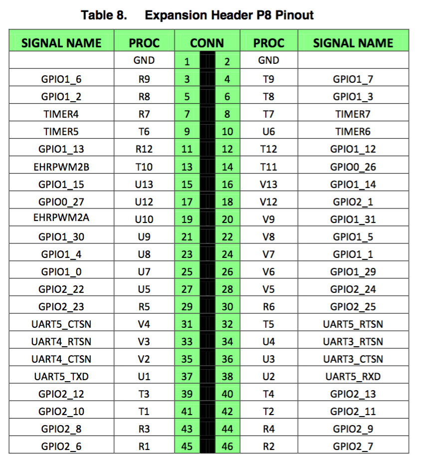
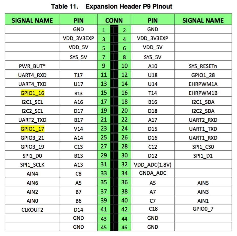
Beaglebone Black has 4 GPIOs 0,1,2,3 the location of each GPIO pin is illustrated at the images below
4.1 Base address
These base address can be find in Memory Map, which is the addresses to be used by OCP.
GPIO_0 0x44E07000
GPIO_1 0x4804C000
GPIO_2 0x481AC000
GPIO_3 0x481AE000
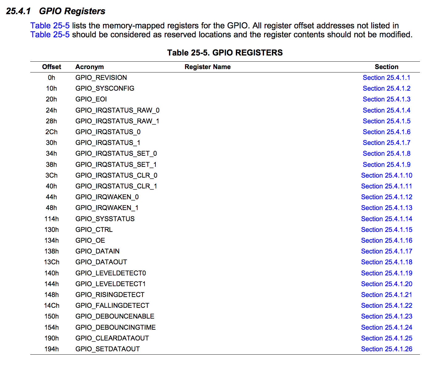
4.2 Registers
Defined in page 4068 of AM335x manual
Which can be defined as a structure in C
struct gpio_csreg {
    volatile uint32 revision;   //0-4
    volatile uint32 res1[3];    //4-10
    volatile uint32 sysconfig;  //10-14
    volatile uint32 res2[3];    //14-20
    volatile uint32 eoi;        //20-24
    volatile uint32 irqstatus_raw_0;//24-28
    volatile uint32 irqstatus_raw_1;//28-2c
    volatile uint32 irqstatus_0;    //2C-30
    volatile uint32 irqstatus_1;    //30-34
    volatile uint32 irqstatus_set_0;//34-38
    volatile uint32 irqstatus_set_1;//38-3c
    volatile uint32 irqstatus_clr_0;//3c-40
    volatile uint32 irqstatus_clr_1;//40-44
    volatile uint32 irqwaken_0; //44-48
    volatile uint32 irqwaken_1; //48-4c
    volatile uint32 res3[50];   //4c-114
    volatile uint32 sysstatus;  //114-118
    volatile uint32 res4[6];    //118-130
    volatile uint32 ctrl;       //130-134
    volatile uint32 oe;         //134-138
    volatile uint32 datain;     //138-13c
    volatile uint32 dataout;        //13c-140
    volatile uint32 leveldetect0;//140-144
    volatile uint32 leveldetect1;//144-148
    volatile uint32 risingdetect;//148-14c
    volatile uint32 fallingdetect;//14c-150
    volatile uint32 debouncenable;//150-154
    volatile uint32 debouncingtime;//154-15c
    volatile uint32 res5[13];   //15c-190
    volatile uint32 cleardataout;   //190-194
    volatile uint32 setdataout;     //194-198
};
The most frequent registers we will use is the oe, datain and dataout.
4.3 GPIO_OE
The GPIO_OE register is used to enable the pins output capabilities. At reset, all the GPIO related pins are configured as input and output capabilities are disabled. This register is not used within the module, its only function is to carry the pads configuration. When the application is using a pin as an output and does not want interrupt generation from this pin, the application can/has to properly configure the Interrupt Enable registers.
4.4 GPIO_IN
The GPIO_DATAIN register is used to register the data that is read from the GPIO pins. The GPIO_DATAIN register is a read-only register. The input data is sampled synchronously with the interface clock and then captured in the GPIO_DATAIN register synchronously with the interface clock. So, after changing, GPIO pin levels are captured into this register after two interface clock cycles (the required cycles to synchronize and to write the data). When the AUTOIDLE bit in the system configuration register (GPIO_SYSCONFIG) is set, the GPIO_DATAIN read command has a 3 OCP cycle latency due to the data in sample gating mechanism. When the AUTOIDLE bit is not set, the GPIO_DATAIN read command has a 2 OCP cycle latency.
4.5 GPIO_OUT
The GPIO_DATAOUT register is used for setting the value of the GPIO output pins. Data is written to the GPIO_DATAOUT register synchronously with the interface clock. This register can be accessed with direct read/write operations or using the alternate Set/Clear feature. This feature enables to set or clear specific bits of this register with a single write access to the set data output register (GPIO_SETDATAOUT) or to the clear data output register (GPIO_CLEARDATAOUT) address.
4.6 GPIO_READ function
For the pinnum(num) to gpio port(gpioN_M) can be calculated by:
num=N*32+M
bool8 GPIO_READ(uint32 PINNUM,bool8 data){
    struct  gpio1_csreg *gpio1ptr;
    uint32 GPIO;
    switch(PINNUM/32){
        case 0:
            GPIO=GPIO_0;
        case 1:
            GPIO=GPIO_1;
        case 2:
            GPIO=GPIO_2;
        case 3:
            GPIO=GPIO_3;
        default:
            GPIO=4;
    }
    if(GPIO==4){
        return SYSERR;
    }
    gpio1ptr = (struct gpio1_csreg *)GPIO;
    uint32 pin=1<<(PINNUM%32);
    //set pin to input
    gpio1ptr->oe |= pin;
    return gpio1ptr->datain>>DHTPIN & 1;
}
4.7 GPIO_WRITE function
syscall GPIO_WRITE(uint32 PINNUM,bool8 data){
    struct  gpio1_csreg *gpio1ptr;
    uint32 GPIO;
    switch(PINNUM/32){
        case 0:
            GPIO=GPIO_0;
        case 1:
            GPIO=GPIO_1;
        case 2:
            GPIO=GPIO_2;
        case 3:
            GPIO=GPIO_3;
        default:
            GPIO=4;
    }
    if(GPIO==4){
        return SYSERR;
    }
    gpio1ptr = (struct gpio1_csreg *)GPIO;
    uint32 pin=1<<(PINNUM%32);
    //set pin to output
    gpio1ptr->oe &= ~pin;
    if(data){
        gpio1ptr->dataout |= pin;
    }else{
        gpio1ptr->dataout &= ~pin;
    }
    return OK;
}


